Phase Change Memory
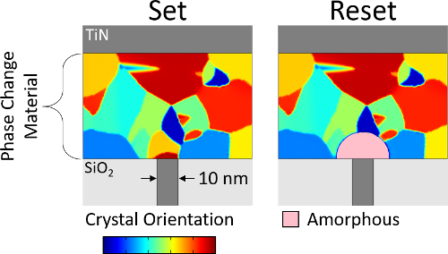
Phase change memory is a nonvolatile memory technology. It stores information as the phase of a material, that is, whether the atoms are aligned in a crystal or display no long-range order (‘amorphous’). The amorphous phase is more resistive; hence, phase can be determined by measuring resistance.
Phase change is achieved by melting and rapidly quenching the device (crystalline-to-amorphous, reset) or by heating the device to a moderate temperature and allowing it to crystallize (amorphous-to-crystalline, set).
Pictured: A phase change mushroom cell in both set and reset configurations. The amorphous mushroom in the reset state increases resistance by >100x.
Finite Element Model
 The finite element method breaks a geometry into small pieces and solves differential equations within each piece to approximate the solution for the whole. This method can be applied to arbitrary geometries where it may be difficult or impossible to obtain an analytic solution, and it allows for different sets of equations to be solved simultaneously and even coupled together.
We have defined a set of differential equations to solve for phase change. We solve for a time-varying ‘crystalline density’ vector (CD), where the magnitude of CD is 1 for the crystalline phase and 0 for the amorphous phase. The orientation of CD corresponds to grain orientation. We capture stochastic nucleation, growth, and melting of discrete grains based on physical models that agree with experimental data. We model phase change device operation by coupling phase change physics with heat transfer and current continuity physics, including temperature and phase dependent material parameters and thermoelectric effects.
Pictured: Polycrystalline anneal at 600 K. The square is 100 nm x 100 nm.
Thermodynamic Parameters
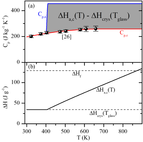 Specific heat is the amount of energy which must be input to a material to increase its temperature. When two phases of a material have different specific heat vs temperature characteristics (like the crystalline and amorphous phases in phase change materials), they contain different amounts of energy at the same temperature. This energy difference is released or absorbed during phase change and is termed the ‘latent heat of phase change.’
The rapid phase transitions at elevated temperatures that make phase change materials useful as memory devices also make it difficult to measure specific heat at these temperatures. However, one can measure the latent heat of phase change (i) during melting and (ii) during crystallization, and the difference in these latent heats gives information about how the specific heat of each phase behaves relative to the other between melting and crystallization.
Pictured:
(Plot) Specific heats for crystalline and amorphous Ge2Sb2Te5 modeled using this method, as well as the resulting latent heat of phase change.
(Animations) Crystal growth and the resulting temperature increase when the latent heat of phase change is included while annealing.
Latent Heat of Phase Change and Specific Heat
![]()
Grain Boundary Melting
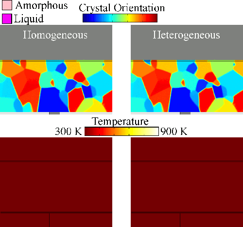 Melting tends to begin at grain boundaries and material interfaces, locations where there is an abnormally high free energy. Crystals shrink as the liquid phase grows, resulting in a transient condition of crystalline islands within a liquid sea before the material is entirely liquid. We model grain boundary melting (‘heterogeneous melting’) in phase change materials and analyze how it impacts device operation.
Grain Boundary Melting Pre-print
Ovonic Threshold Switching
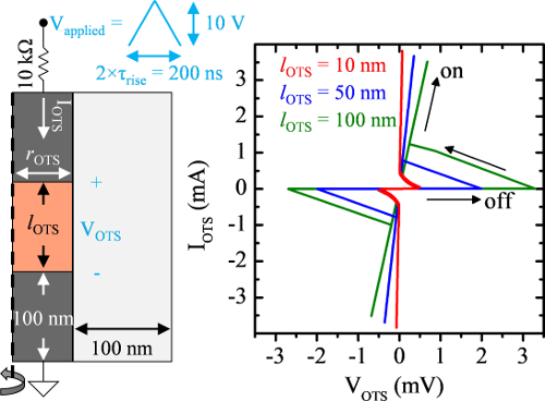 Certain amorphous semiconductors switch from low-conductivity to high-conductivity when exposed to a sufficiently high electric field. The field may drop even as current increases once switching begins, resulting in a characteristic I-V ‘s-curve’. This phenomenon was first observed by Ovshinsky in the late 60’s and is termed ‘ovonic threshold switching’. Despite many studies since, the mechanism(s) behind ovonic switching are poorly understood due to the complex coupling between electrical and thermal contributions to conductivity in devices with a ‘dirty’ bandgap like amorphous semiconductors. Several models have been proposed in recent years, all claiming to capture the I-V characteristics observed in ovonic switches.